This is the ATF1508 I use mostly.. You can see the GCLK (global clock) at the bottom and that its on a "global bus" between all logic cells.

- Capture.JPG (59.08 KiB) Viewed 2753 times
A breakdown of a cell.. See global bus at the bottom..
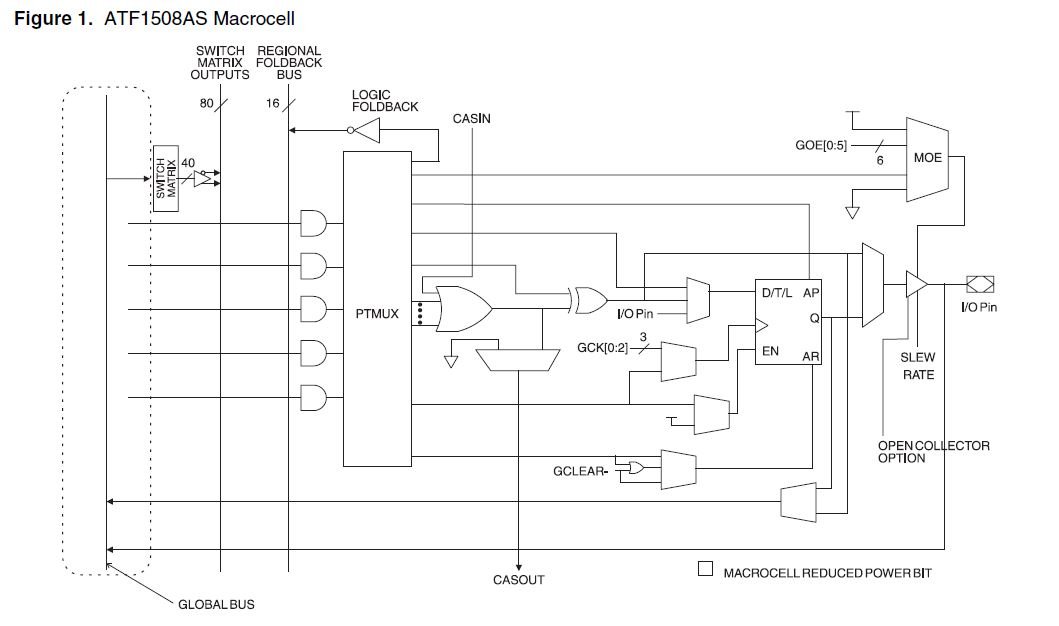
- 2.JPG (56.71 KiB) Viewed 2753 times
I guess you have to imagine global clocks as going to every flipflip in the PLD. Its hardwired , so doesn't take up much space.
OTOH, if you used a different clock input, the compiler would have to route that to every cell its used on..
Take the humbal 22V10 layout..

- 3.JPG (57.91 KiB) Viewed 2753 times
Now imagine the chaos to route clocks to cells via this array..
Note pin 1 is the global clock pin on the 22V10..

- 4.JPG (163.75 KiB) Viewed 2753 times
The path from any input pin to a cell Can quite literally be chaos across the array.. Add in a few more clocks to various "random" cells and you end up with a right sh*t sandwich

So using the global clock pins pretty much means the routing is "free" as its already hardwired across the global bus.


