Next update in my journey towards a desk-mounted-smoke-generator...
There are a bunch of mysterious things on the board (some more mysterious than others) which need de-confused before I can put this near my Atari.
The PAL chip was the most concerning part because if I do something wrong and blow it up, I can't replace it. It might also be a show-stopper for using the board at all, without cutting lots of traces and using it as a convenient peg-board instead of its intended topology with the VME connections etc.

- pal.jpg (634.71 KiB) Viewed 47 times
There are also 3 ICs marked DM1/DM2/DM3 which have the part number SN74S1057SC.
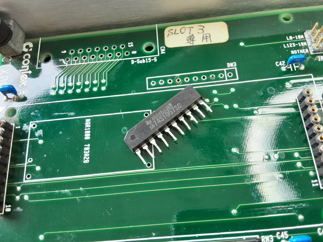
- mystery-buffer.jpg (320.3 KiB) Viewed 47 times
Searching for this produced results ranging from 'vague' to 'not even close, thanks'. I managed to trace out what these are connected to but results did not make much obvious sense. It was wired as if operating as a buffer for inputs but seemed to be exposing both buffered and unbuffered versions of the same signals on the external connector.
Will come back to this one later.
There are three 74BCT244 buffers on the board tied to a bank of resistors. With some DMM probing I mapped some of these to the external VME P2 connector and to links on the TRAM slots so those are there to buffer link signals on the bus.

- buffers.jpg (636.26 KiB) Viewed 47 times
Given the total number of connections on the board I did not probe everything exhaustively but took samples from various places to try to build up a pattern of which things were handling which signals and especially numbering patterns that could allow me to predict the un-probed ones.
I started the process using a wire-wool cleaning sponge as the 'search' probe with the other probe either at GND, VCC or some point of interest. This narrowed things down quickly. I could change the sponge to a 1cm metal brush to sweep pin rows more easily and find where on the row the signal was.
There are several jumpers on the board, all clearly marked. The meaning of some could be (partly) figured out directly from the markings, some pretty vague and I had to guess and probe around a bit.

- jumpers.jpg (663.76 KiB) Viewed 47 times
JP3-JP8 are adjacent to some of the TRAMs and the markings (Lxy) seem to point at making/breaking links between them or exposing them to the VME - which would make sense.
JP9 is ore of a 'global settings' switch to set serial link speed for some links and may configure the board in a master/slave config from the VME perspective.
Next update will show what I found from the probing, what those DM1/2/3 chips are, what the PAL is actually doing and begin to build up a topology....