Page 1 of 5
ST FPGA MMU Development
Posted: 19 Jan 2020 16:44
by Icky
We have been talking about the FPGA MMU for some time in the Blitter recreation thread -
https://www.exxosforum.co.uk/forum/view ... 280#p29329 and I have finally found some time to sort out the boards we have, so thought I would start a thread just for the MMU development.
Replacing the funky socket with header sockets enables the ability to plug in one of
@exxos funky to PLCC adaptors to make sure the original MMU still works.
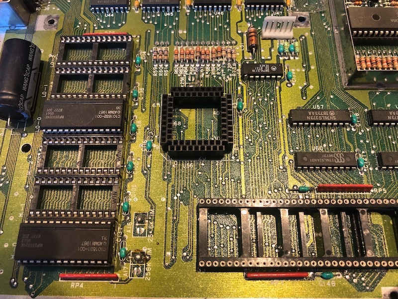
- IMG_4757.jpeg (328.09 KiB) Viewed 8972 times
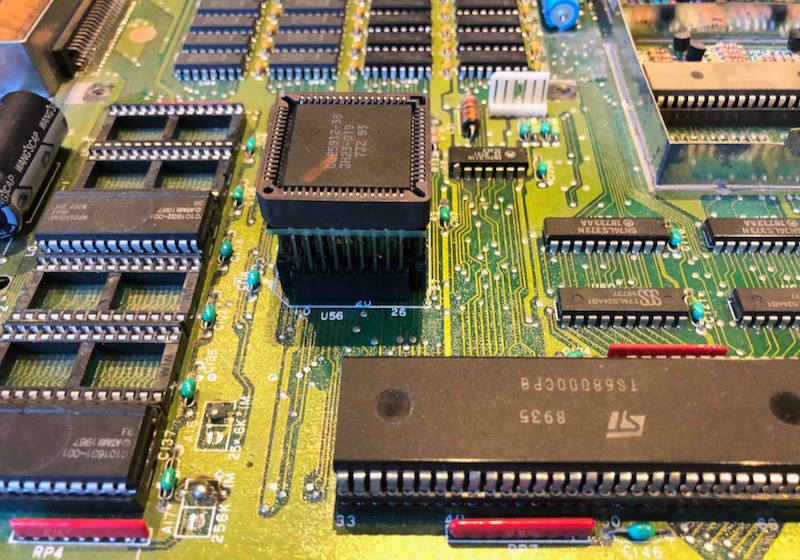
- IMG_4762.jpeg (224.2 KiB) Viewed 8972 times
This also allows the Shock Absorber 5V <-> 3.3V funky socket buffer board to be put in place then an FPGA dev board on top.
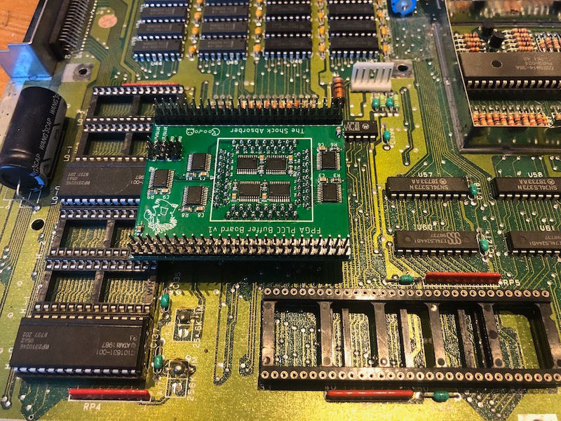
- IMG_4758.jpeg (317.74 KiB) Viewed 8972 times
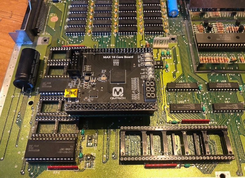
- IMG_4759.jpeg (265.55 KiB) Viewed 8972 times
Now the DEV STFM board is ready for MMU testing once we get the firmware sorted.
EDIT: For reference is a link to the MMU Pinout from the IC section on the forum

Re: ST FPGA MMU Development
Posted: 19 Jan 2020 16:56
by exxos
Ooo nice :)
Re: ST FPGA MMU Development
Posted: 19 Jan 2020 17:27
by PhilC
Just as I was missing the stacking boards ever present on the Alpha, along comes @Icky to fulfill the void :D
Re: ST FPGA MMU Development
Posted: 19 Jan 2020 17:37
by exxos
@Icky was the power pins in the same place as the blitter ? cant remember now..
Re: ST FPGA MMU Development
Posted: 19 Jan 2020 17:50
by Icky
exxos wrote: 19 Jan 2020 17:37
@Icky was the power pins in the same place as the blitter ? cant remember now..
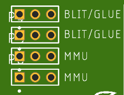
There are slight variations in power pins between Blitter, MMU and GLUE. The Shock Absorber has 4 sets of jumpers that switches the correct pins around. It can be used for all three chips.
- Screenshot 2020-01-19 at 17.47.17.png (14.35 KiB) Viewed 8947 times
Re: ST FPGA MMU Development
Posted: 19 Jan 2020 18:00
by exxos
Icky wrote: 19 Jan 2020 17:50
There are slight variations in power pins between Blitter, MMU and GLUE. The Shock Absorber has 4 sets of jumpers that switches the correct pins around. It can be used for all three chips.
oh cool , flash with suska core and job done :lol:
Re: ST FPGA MMU Development
Posted: 19 Jan 2020 18:03
by Icky
@exxos - thats the plan. Just doing the pin planner now but need some food :) so hopefully might see some progress later.
Re: ST FPGA MMU Development
Posted: 08 Feb 2020 18:43
by Icky
So an update on the FPGA MMU. Firstly thanks to Wolfgang (Suska) for helping with the original MMU code minus all the STE enhancements.
We have two of these FPGA buffer / dev kit board combos. I have one and
@exxos the other.
I have managed to eventually get the board to boot running as an MMU and I can run things like GB6.
@exxos however, his board wouldn't play ball and has sent back to me to test and it looks like something is not right with the buffer board so will replace and send back. It did however create some pretty crash screens :)
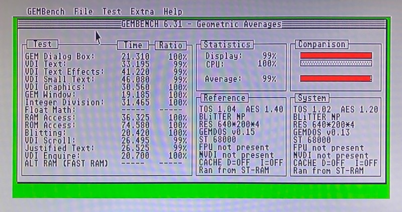
Now this is in no way a solid solution as we have noticed various things that will need to be fixed to make this work properly. Below is a screenshot of GB6 I ran. Its not an exact comparison as the on board ROMs on my DEV ST MB are 102.
- IMG_4771.jpeg (152.98 KiB) Viewed 8820 times
The next test after GB6 was the Closure demo and this is where the MMU is tripping up as the demo crashes. Our goal is to get to a point with the firmware where the Closure demo runs, so our FPGA MMU saga continues :)
Re: ST FPGA MMU Development
Posted: 08 Feb 2020 19:27
by PhilC
Good to see you've got this far :dualthumbup:
Re: ST FPGA MMU Development
Posted: 09 Feb 2020 15:43
by exxos
I wonder if @troed can shed any light on how the wakeup states are detected ? As Closure doesn't detect any and doesn't run...