Page 43 of 69
Re: The Cosmic Puppet's Universe.
Posted: 25 Jun 2022 00:09
by Cosmic Puppet

- 20220625_000312.jpg (194.54 KiB) Viewed 1903 times
These are quite short which might work jewellery wise. Any idea what the circles are for? Wondering if they could be used as an attachment point on the back-side.
Re: The Cosmic Puppet's Universe.
Posted: 25 Jun 2022 00:17
by exxos
Cosmic Puppet wrote: 25 Jun 2022 00:09
Any idea what the circles are for? Wondering if they could be used as an attachment point on the back-side.
Never thought about it :lol: Assume used as alignment points for assembly machines.
Still don't get why Atari used those mask roms over eproms. Unless they were simply cheaper.
Re: The Cosmic Puppet's Universe.
Posted: 25 Jun 2022 00:30
by Cosmic Puppet
exxos wrote: 25 Jun 2022 00:17
Cosmic Puppet wrote: 25 Jun 2022 00:09
Any idea what the circles are for? Wondering if they could be used as an attachment point on the back-side.
Never thought about it :lol: Assume used as alignment points for assembly machines.
Still don't get why Atari used those mask roms over eproms. Unless they were simply cheaper.
What's a mask rom?
Re: The Cosmic Puppet's Universe.
Posted: 25 Jun 2022 00:34
by exxos
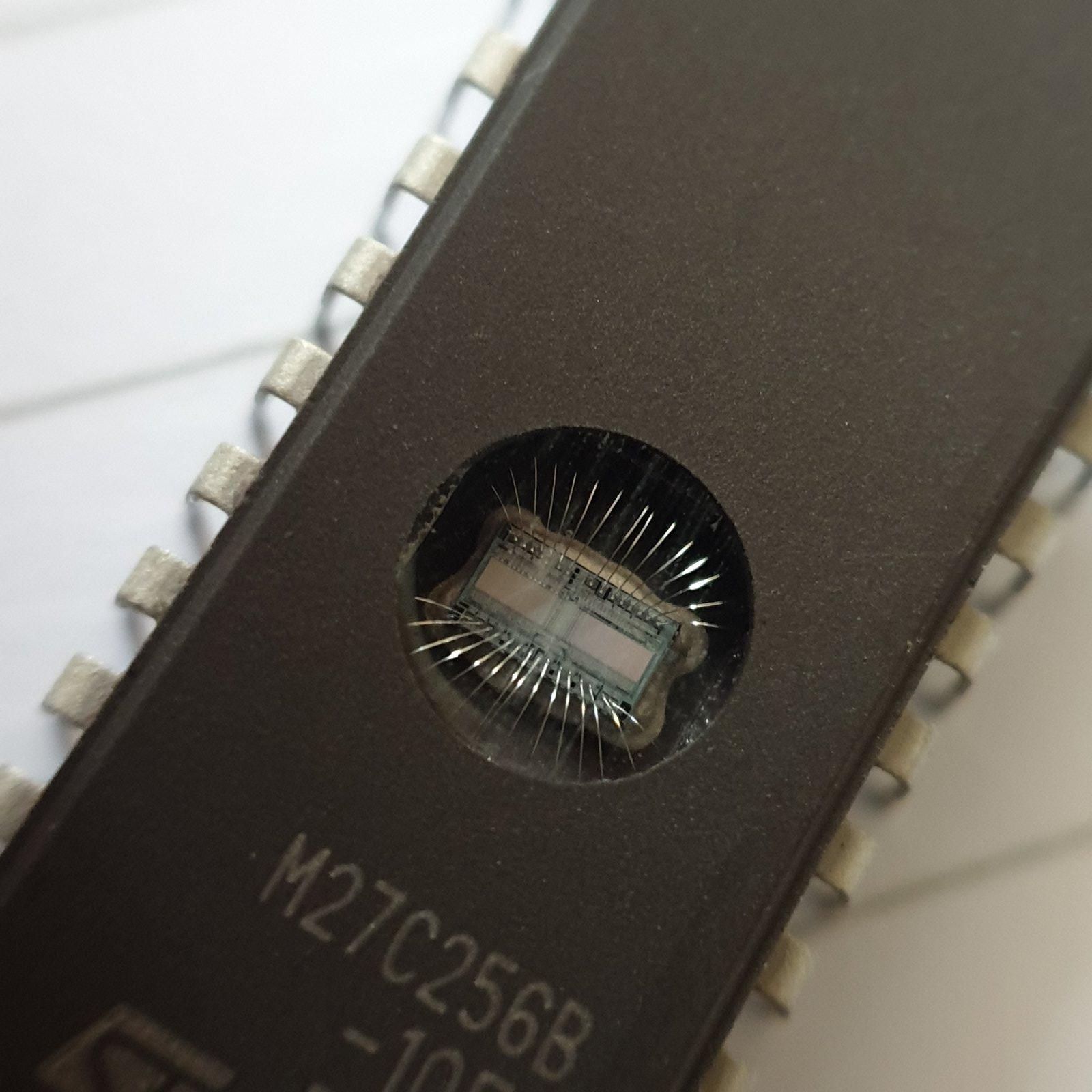
Those ROM chips are.. One time programmable.. Eproms had a little window so you could erase them.. Is assume they be more common and mass produced and cheaper.. But couldn't have been.
Re: The Cosmic Puppet's Universe.
Posted: 25 Jun 2022 01:03
by Cosmic Puppet
- 20190804_124234.jpg (214.97 KiB) Viewed 1890 times
Re: The Cosmic Puppet's Universe.
Posted: 25 Jun 2022 12:19
by stephen_usher
exxos wrote: 25 Jun 2022 00:34
Those ROM chips are.. One time programmable.. Eproms had a little window so you could erase them.. Is assume they be more common and mass produced and cheaper.. But couldn't have been.
Usually "Mask ROMs" use the technique of setting the content of the ROM during chip manufacture, using one of the optical "masks" to encode the data.
Once the costly process of making the original optical mask is done the price per unit for a large batch is small as after the wafer is produced there's only the standard chip testing and encapsulation to do. There's no separate, and expensive, programming step involved.
Re: The Cosmic Puppet's Universe.
Posted: 25 Jun 2022 12:21
by Cosmic Puppet
stephen_usher wrote: 25 Jun 2022 12:19
exxos wrote: 25 Jun 2022 00:34
Those ROM chips are.. One time programmable.. Eproms had a little window so you could erase them.. Is assume they be more common and mass produced and cheaper.. But couldn't have been.
Usually "Mask ROMs" use the technique of setting the content of the ROM during chip manufacture, using one of the optical "masks" to encode the data.
Once the costly process of making the original optical mask is done the price per unit for a large batch is small as after the wafer is produced there's only the standard chip testing and encapsulation to do. There's no separate, and expensive, programming step involved.
Cool.
I was also thinking this morning is an IC just miniature version of a circuit?
Re: The Cosmic Puppet's Universe.
Posted: 25 Jun 2022 12:24
by Cosmic Puppet
It's happening @exxos DMA is at the jewellers being made into a custom piece of jewellery with a new 1 inch shorter chain. He's totally on the ball with a way to do it.
Mad thing is the preferred DMA for STEs costs more to buy on eBay than my piece of jewellery.
Re: The Cosmic Puppet's Universe.
Posted: 25 Jun 2022 12:29
by exxos
Cosmic Puppet wrote: 25 Jun 2022 12:21
I was also thinking this morning is an IC just miniature version of a circuit?
Yep. Individual transistors are large. In a IC you can have zillions of them in there.
Its why PLDs are cool. Like GAL chips. If a circuit was built out of logic chips it could he large and a pain to make corrections. So being able to put gates inside a single GAL chip means instead of track cutting and bodge wires, you fan change it all in software.
EG if you had 2 buffers in series, they could be in 1 logic IC. But oh crap now you need a buffer and inverter, so you have to bodge a extra chip on the PCB. In a GAL you can add a inverter in seconds. No PCB changes needed. Being able to do custom logic is a huge saving in logic chips and PCB space. Your PCB is basically in software.
Re: The Cosmic Puppet's Universe.
Posted: 25 Jun 2022 12:41
by Cosmic Puppet
exxos wrote: 25 Jun 2022 12:29
Cosmic Puppet wrote: 25 Jun 2022 12:21
I was also thinking this morning is an IC just miniature version of a circuit?
Yep. Individual transistors are large. In a IC you can have zillions of them in there.
Its why PLDs are cool. Like GAL chips. If a circuit was built out of logic chips it could he large and a pain to make corrections. So being able to put gates inside a single GAL chip means instead of track cutting and bodge wires, you fan change it all in software.
EG if you had 2 buffers in series, they could be in 1 logic IC. But oh crap now you need a buffer and inverter, so you have to bodge a extra chip on the PCB. In a GAL you can add a inverter in seconds. No PCB changes needed. Being able to do custom logic is a huge saving in logic chips and PCB space. Your PCB is basically in software.
I don't understand all that technical stuff but I can see now why the first computers were so large.
p.s. War Games is on Film 4 at 12:50pm Bit of eighties nostalgia and a big ass computer called WOPR.
I was reading a thing about CPUs and it said "They contain billions of transistors" and I thought, "No, sixty eight thousand" :lol: